The issue of electromagnetic interference (EMI) in design has always been a headache, especially in the automotive industry. In order to minimize electromagnetic interference as much as possible, designers usually reduce noise sources by reducing the high di/dt loop area and switch conversion rate when designing schematic diagrams and drawing layouts.
However, sometimes, no matter how cautious the layout and schematic design may be, it is still not possible to reduce the conducted EMI to the required level. This is because noise is not only dependent on circuit parasitic parameters, but also on current intensity. In addition, the opening and closing actions of the switch will generate discontinuous currents, which will generate voltage ripples on the input capacitor, thereby increasing EMI.
Therefore, it is necessary to adopt some other methods to improve the performance of conducted EMI. This article mainly discusses introducing an input filter to filter out noise, or adding a shielding cover to lock in noise.
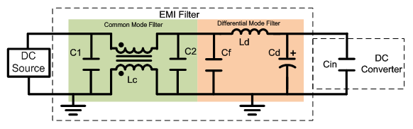
Figure 1 Schematic diagram of EMI filter
Figure 1 shows a simplified EMI filter, including a common mode (CM) filter and a differential mode (DM) filter. Usually, DM filters are mainly used to filter out noise below 30MHz (DM noise), while CM filters are mainly used to filter out noise between 30MHz and 100MHz (CM noise). But in fact, these two filters have a certain inhibitory effect on EMI noise throughout the entire frequency band.
Figure 2 shows an input lead noise without a filter, including positive and negative noise, and the peak and average levels of these noises are labeled. Among them, the tested system mainly uses chip LMR14050SSQDDARQ1 to output 5V/5A, and supplies power to subsequent chips TPS65263QRHBRQ1, while outputting 1.5V/3A, 3.3V/2A, and 1.8V/2A. Both chips operate at a switching frequency of 2.2MHz.
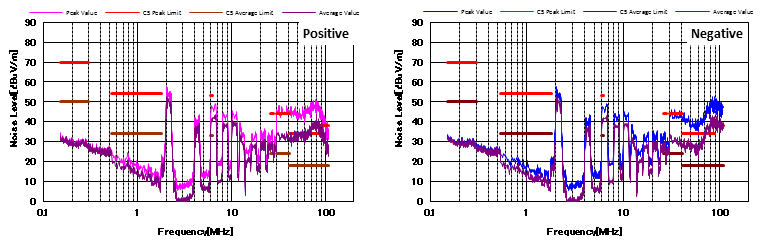
Figure 2 Noise characteristics under C5 standard (without filter)
Figure 3 shows the EMI results after adding a DM filter. From the figure, it can be seen that the DM filter attenuates the mid frequency band DM noise (2MHz to 30MHz) by nearly 35dB μ V/m. In addition, the high-frequency noise (30MHz to 100MHz) has also decreased, but still exceeds the limit level. This is mainly because the DM filter has limited filtering ability for high-frequency CM noise.

Figure 3 Noise characteristics under C5 standard (with DM filter)
Figure 4 shows the noise characteristics after adding CM and DM filters. Compared to Figure 3, the increase in CM filter reduces by nearly 20dB μ CM noise of V/m. And EMI performance has also passed the CISPR25 C5 standard.

Figure 4 Noise characteristics under C5 standard (with CM and DM filters)
Figure 5 shows the noise characteristics with CM and DM filters under different layouts, where the filter is the same as Figure 4. But compared to Figure 4, the noise in the entire frequency band has increased by approximately 10dB μ V/m, high-frequency noise even exceeds the average value of the CISPR25 C5 standard.
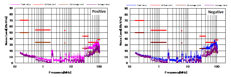
Figure 5 Noise characteristics under C5 standard (with CM and DM filters, different layouts)
The difference in noise results between Figure 4 and Figure 5 is mainly due to differences in PCB wiring, as shown in Figure 6. In the wiring of Figure 5 (on the right side of Figure 6), a large area of copper clad (GND) surrounds the DM filter and forms some parasitic capacitors with Vin wiring. These parasitic capacitors provide an effective low impedance path for high-frequency signal bypass filters. Therefore, in order to maximize the performance of the filter, it is necessary to remove all copper cladding around the filter, as shown in the wiring on the left side of Figure 6.
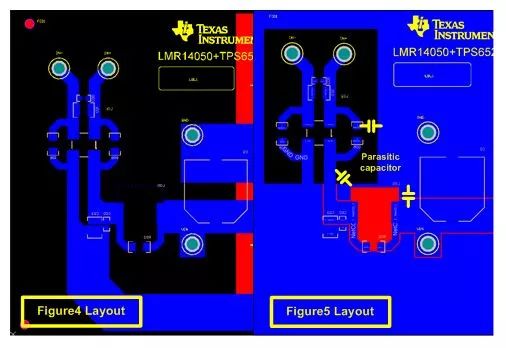
Figure 6 Different PCB Wiring
In addition to adding filters, another effective way to optimize EMI performance is to add shielding covers. This is because the metal shield connected to GND can prevent noise from radiating outward. Figure 7 recommends a placement method for the shielding cover. The shielding cover exactly covers all the components on the board.
Figure 8 shows the EMI results after adding a filter and shielding cover. As shown in the figure, almost all the noise in the entire frequency band is eliminated by the shielding cover, resulting in excellent EMI performance. This is mainly because the long input leads, which are equivalent to antennas, can couple a large amount of radiated noise, and the shielding shield precisely isolates them. In this design, intermediate frequency noise will also be coupled to the input lead in this way.
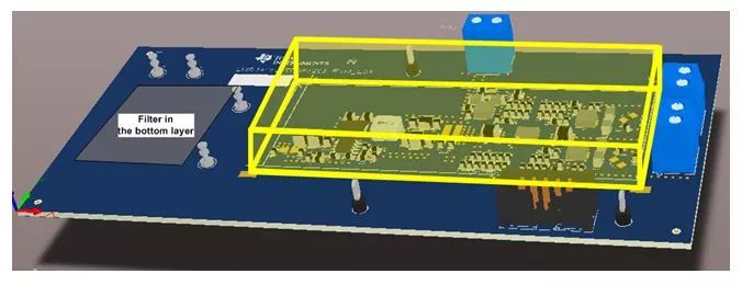
Figure 7 3D Model of PCB with Shielding Cover
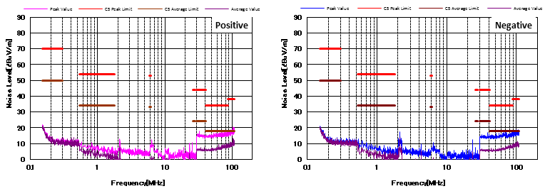
Figure 8 Noise characteristics under C5 standard (with CM, DM filters, and shielding cover)
Figure 9 also shows the noise characteristics with filters and shielding. Unlike Figure 8, the shielding case in Figure 9 is a metal box that wraps the entire circuit board and only the input leads are exposed outside. Although this shield is present, some radiated noise can still bypass the EMI filter and couple to the power line on the PCB, which will result in worse noise characteristics than shown in Figure 8. Interestingly, the noise characteristics of the high-frequency bands in Figures 4, 8, and 9 (with the same layout and wiring) are almost identical. This is because after adding an EMI filter, the high-frequency radiated noise that can be coupled to the input line almost disappears.
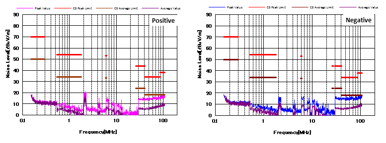
Figure 9 Noise characteristics under C5 standard (with CM, DM filters, and shielded metal box)
Post time: Jul-05-2023


